
공부중
[DSM] 논문 : Sigma-Delta Modulators (1) Introduction 본문
[DSM] 논문 : Sigma-Delta Modulators (1) Introduction
복습 2024. 9. 10. 00:50Sigma-Delta Modulators: Tutorial Overview, Design Guide, and State-of-the-Art Survey
(1) Introduction
(2) Fundamentals of ΣΔ Modulators
A. Oversampling
B. Quantization Error and White Noise Model
C. Noise Shaping
0. 초록(Abstract)
Abstract:
요약: 이 논문은 ΣΔ 변조기의 작동 원리와 구조, 회로 오류와 모델, 설계 방법, 그리고 실제 문제에 대한 개관을 설명합니다. 나노미터 CMOS 구현에 대한 최신 기술을 리뷰하며, 차세대 무선 통신 시스템에의 응용을 강조한 최첨단 ΣΔ 구조에 대한 조사를 제공합니다.
Introduction
Since the first idea underlying the operation of ΣΔ modulators (ΣΔMs) was patented [1] and applied to implement analog-to-digital converters (ADCs) [2] around 50 years ago, there has been a huge number of circuits and systems exploiting ΣΔMs in many different industrial applications—from instrumentation to communications [3]–[16]. Based on the combination of oversampling and quantization error shaping techniques, ΣΔMs achieve a high degree of insensitivity to analog circuit imperfections, thus making them a good choice (the best one in many cases) to realize embedded analog-to-digital interfaces in modern systems-on-chip (SoCs) integrated in nanometer CMOS.
ΣΔ 변조기(ΣΔMs)의 기본 개념이 특허를 받고 [1], 약 50년 전에 아날로그-디지털 변환기(ADCs) [2]를 구현하는 데 적용된 이래, 많은 다양한 산업 분야에서 ΣΔMs를 활용하는 회로 및 시스템이 대거 등장했습니다—측정 기기에서 통신에 이르기까지 [3]–[16]. 오버샘플링과 양자화 오류 형성 기술의 조합을 기반으로, ΣΔMs는 아날로그 회로의 불완전성에 대한 높은 무관심을 달성하여, 이로 인해 많은 경우 최상의 선택이 되며, 나노미터 CMOS에서 통합된 현대 시스템온칩(SoCs) 내에 내장된 아날로그-디지털 인터페이스를 구현하는 데 좋은 선택이 됩니다.
In spite of the aforementioned advantages, the design of CMOS ΣΔMs involves a number of practical issues and trade-offs that must be taken into account in order to optimize their performance in terms of power consumption, silicon area, and time-to-market deployment. Over the last few years, significant efforts have been made to decrease the power budget and to increase the speed of ΣΔMs, while simultaneously maintaining compatibility with mainstream digital technologies.
앞서 언급한 장점에도 불구하고, CMOS ΣΔMs의 설계는 전력 소비, 실리콘 면적, 시장 출시 시간 측면에서 그 성능을 최적화하기 위해 고려해야 할 여러 실제 문제와 타협점을 포함합니다. 지난 몇 년 동안 ΣΔMs의 전력 예산을 줄이고 속도를 높이는 데 상당한 노력이 기울여졌으며, 동시에 주류 디지털 기술과의 호환성을 유지하고 있습니다.
This paper presents a broad survey of ΣΔMs,1 the new advances and trends in architectures, circuit techniques, design methodologies, and practical considerations, with emphasis on nanometer CMOS realization. The paper is organized as follows. Section II gives a brief background regarding fundamentals of ADCs and basic concepts underlying ΣΔMs. Section III surveys the basic ΣΔM architectures and Section IV describes their main building blocks, error mechanisms as well as the application of their analysis and models to the development of design methodologies. Finally, Section V sums up the state-of-the-art performance, trends, and challenges.
이 논문은 ΣΔ 변조기들의 넓은 조사, 새로운 발전과 구조, 회로 기술, 설계 방법론 및 실제 고려 사항들을 소개하며, 특히 나노미터 CMOS 실현에 중점을 둡니다. 논문은 다음과 같이 구성되어 있습니다. 제2장에서는 ADCs의 기본 원리와 ΣΔMs의 기본 개념에 대해 간략히 설명합니다. 제3장에서는 기본적인 ΣΔM 구조를 조사하고, 제4장에서는 주요 구성 요소, 오류 메커니즘 및 설계 방법론 개발을 위한 분석 및 모델 적용을 설명합니다. 마지막으로, 제5장에서는 최신 성능, 추세 및 도전 과제를 정리합니다.
Fundamentals of ΣΔ Modulators
Fundamentals of ΣΔ Modulators
The operation of ΣΔMs relies on the combination of two signal processing techniques, namely: oversampling and quantization error filtering and feedback, commonly referred to as noise shaping. Both techniques are related to the fundamental processes involved in an ADC—illustrated in Fig. 1.
제2장. ΣΔ 변조기의 기본 원리
ΣΔ 변조기(ΣΔMs)의 작동은 두 가지 신호 처리 기술, 즉 오버샘플링과 양자화 오류 필터링 및 피드백의 조합에 의존하며, 이는 일반적으로 노이즈 셰이핑으로 불립니다. 이 두 기술은 ADC에 관련된 기본적인 과정과 관련이 있으며, 그 과정은 그림 1에서 설명됩니다.
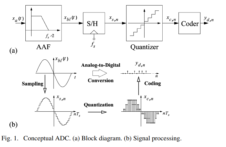
Fig. 1(a) shows the conceptual scheme of an ADC intended for the digitization of low-pass (LP) signals, that includes the following components: an anti-aliasing filter (AAF), a sampling-and-hold (S/H) circuit, a quantizer, and a coder [17]. The operation of these blocks is illustrated in Fig. 1(b). First, the analog input signal, xa(t), passes through the AAF block. Otherwise, from the Nyquist sampling theorem, high frequency components of the input signal would be folded or aliased into the signal bandwidth, Bw, thus corrupting the signal information [18]. The resulting band-limited signal, xbl(t), is sampled at a rate of fs by the S/H circuit, thus yielding a discrete-time (DT) signal,2 xs,n=xbl(nTs). Following the S/H, the quantizer maps the continuous range of amplitudes of xs,n into a discrete set of levels. Finally, the coder assigns a unique binary number to each level providing the output digital data. Therefore, as illustrated in Fig. 1(b), the fundamental processes involved in an ADC are: sampling and quantization. These two continuous-to-discrete transformations limit the performance of ADCs [18].
A. Oversampling
A. Oversampling
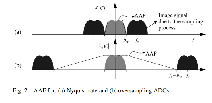
The sampling process imposes a limit on Bw, and hence on the speed of the ADC. According to the Nyquist theorem, which sets that the minimum value of fs—often referred to as Nyquist frequency and represented by fN—must be twice the signal bandwidth, i.e., fN=2Bw. Based on this criterion, those ADCs with fs=fN are called Nyquist-rate ADCs, while if fs>fN, the resulting ADCs are known as oversampling ADCs, and OSR≡fs/fN is defined as the oversampling ratio [5]. One of the advantages of oversampling ADCs is that they simplify the requirements placed on the AAF as illustrated in Fig. 2. Note that the AAF for a Nyquist converter must have a sharp transition band, which often introduces phase distortion in signal components located near the cut-off frequency.
A. 오버샘플링
샘플링 과정은 Bw에 한계를 부과하며, 따라서 ADC의 속도에도 영향을 미칩니다. 나이퀴스트 정리에 따르면, fs의 최소값—일반적으로 나이퀴스트 주파수라고 하며 fN으로 표현됩니다—는 신호 대역폭의 두 배, 즉 fN=2Bw여야 합니다. 이 기준에 따라 fs=fN인 ADC는 나이퀴스트율 ADC라고 불리며, fs>fN인 경우 결과적으로 생성되는 ADC는 오버샘플링 ADC로 알려져 있고, OSR≡fs/fN은 오버샘플링 비율로 정의됩니다 [5]. 오버샘플링 ADC의 장점 중 하나는 그림 2에서 보여주듯이 AAF에 대한 요구 사항을 단순화한다는 것입니다. 나이퀴스트 변환기의 AAF는 급격한 전환 대역을 가져야 하며, 이는 종종 컷오프 주파수 근처에 위치한 신호 성분에 위상 왜곡을 도입합니다.
B. Quantization Error and White Noise Model
The quantization itself introduces a fundamental limitation on the performance of an ideal ADC. It degrades the quality of the input signal whose continuous-value levels are mapped onto a finite set of discrete levels as illustrated in Fig. 3. This continuous-to-discrete transformation in amplitude generates an error, commonly referred to as quantization error. Contrary to the sampling process, quantization is a nonreversible operation, causing a loss in the resolution of the digitized signal [18].
B. 양자화 오류와 백색 잡음 모델 양자화 자체는 이상적인 ADC의 성능에 대한 근본적인 제한을 도입합니다. 이는 연속적인 값 수준의 입력 신호가 유한한 이산 수준 집합으로 매핑되면서 품질이 저하되는데, 이는 그림 3에서 보여주듯이 발생합니다. 이 연속에서 이산으로의 진폭 변환은 일반적으로 양자화 오류라고 불리는 오류를 생성합니다. 샘플링 과정과는 달리, 양자화는 비가역적인 작업으로, 디지털화된 신호의 해상도 손실을 초래합니다 [18].
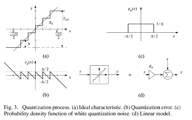
Fig. 3(a) shows the transfer characteristic of an ideal quantizer, where gq denotes the slope of the line intersecting the code steps or quantizer gain, and eq(x) stands for the quantization error. This error is a nonlinear function of the input signal, x, as shown in Fig. 3(b). Note that, if x is confined to the full-scale input range [−XFS/2,XFS/2], the quantization error is bounded by [−Δ/2,Δ/2], with Δ being the quantization step, defined as the separation between adjacent output levels in the quantizer. For a B-bit quantizer, the quantization step is defined as Δ≡YFS/(2B−1), with YFS being the full-scale output range of the quantizer [see Fig. 3(a)]. For inputs outside of the interval [−XFS/2,XFS/2], the absolute value of eq(x) exceeds Δ/2 and grows monotonically. This situation is known as overloading of the quantizer [5]–[7].
그림 3(a)는 이상적인 양자화기의 전달 특성을 보여주며, 여기서 gq는 코드 단계를 교차하는 선의 기울기 또는 양자화기의 이득을 나타내고, eq(x)는 양자화 오류를 나타냅니다. 이 오류는 그림 3(b)에서 보여주듯이 입력 신호 x의 비선형 함수입니다. x가 전체 스케일 입력 범위 [−XFS/2, XFS/2]에 국한되면, 양자화 오류는 [−Δ/2, Δ/2]에 의해 제한되며, 여기서 Δ는 인접한 출력 레벨 사이의 분리로 정의되는 양자화 단계입니다. B비트 양자화기의 경우, 양자화 단계는 Δ≡YFS/(2^B−1)로 정의되며, 여기서 YFS는 양자화기의 전체 스케일 출력 범위입니다 [그림 3(a) 참조]. 입력이 [−XFS/2, XFS/2] 구간을 벗어날 경우, eq(x)의 절대값은 Δ/2를 초과하고 단조롭게 증가합니다. 이 상황은 양자화기의 과부하로 알려져 있습니다 [5]–[7].
As shown in Fig. 3(b), eq(x) strongly depends on x. However, under some assumptions which are normally met in practice [19]–[22], it can be shown that the quantization error distributes uniformly in the range [−Δ/2,Δ/2], with rectangular probability density, ρq(eq), shown in Fig. 3(c), having a constant power spectral density (PSD) [19]. Because of that, the quantization error can be modeled as an additive white noise source, e, as shown in Fig. 3(d), usually called quantization noise.3 As the total quantization noise power, σ2(e), is uniformly distributed in the range [−fs2,fs/2], its 2-sided PSD is given by
{S_E(f)} \!\equiv\! {\sigma^2(e) \over f_s}\!=\!{1 \over f_{s}}\left[{1 \over \Delta}\int_{-\Delta/2}^{\Delta/2} e^2de\right]\!=\!{\Delta^2 \over 12f_s} \quad\eqno{\hbox{(1)}}
and the in-band noise power, calculated for LP signals as 4
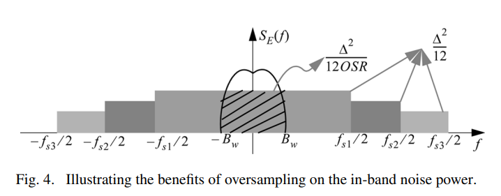
{P_E} \equiv \int_{-B_{w}}^{B_{w}} S_{E}(f)df={\Delta^2 \over 12{\hbox{OSR}}} \eqno{\hbox{(2)}}
decreases with OSR at a rate of 3 dB/octave. This property is exploited by oversampling ADCs, since when an oversampled signal is quantized, the spectral components of the quantization error are distributed in a larger frequency band as illustrated in Fig. 4, thus attenuating the in-band quantization noise power as compared to the one achieved by Nyquist-rate ADCs.
그림 3(b)에서 보여주듯이, eq(x)는 x에 크게 의존합니다. 그러나 실제에서 일반적으로 만족되는 일부 가정하에 [19]–[22], 양자화 오류가 [−Δ/2, Δ/2] 범위에서 균등하게 분포하며, 그림 3(c)에서 보여지는 사각 확률 밀도, ρq(eq)를 가지고 상수 전력 스펙트럼 밀도(PSD)를 가짐을 보일 수 있습니다 [19]. 이 때문에, 양자화 오류는 그림 3(d)에서 보여지듯이, 일반적으로 양자화 잡음이라고 불리는 가산 백색 잡음원, e,으로 모델링될 수 있습니다. 전체 양자화 잡음의 전력, σ^2(e),가 [−fs/2, fs/2] 범위에서 균등하게 분포하므로, 그 양면 PSD는 다음과 같이 주어집니다:
밴드 내 잡음 전력은 저역통과(LP) 신호에 대해 계산되며, 공식은 다음과 같습니다:
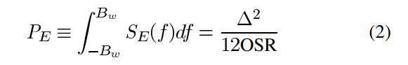
이것은 OSR이 증가함에 따라 3 dB/옥타브의 비율로 감소합니다. 이 속성은 오버샘플링 ADC에 의해 활용됩니다. 오버샘플된 신호가 양자화될 때, 양자화 오류의 스펙트럼 성분들이 더 큰 주파수 대역에 분포하게 되며, 그림 4에서 보여지듯이, 이는 나이퀴스트율 ADC에 의해 달성된 것과 비교하여 밴드 내 양자화 잡음 전력을 감소시킵니다.
C. Noise Shaping
C. Noise Shaping
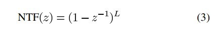
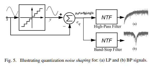
The accuracy of an oversampling ADC can be further increased by filtering the quantization noise in such a way that most of its power lies outside the signal band. This is illustrated in Fig. 5, where the quantization error—conceptually generated from substracting the input signal, x, from an analog version of the quantizer output, y—is shaped by a filter with a transfer function, usually called noise transfer function (NTF), which can be either of high-pass type [Fig. 5(a)] or band-stop type [Fig. 5(b)], respectively filtering the noise around either dc or at a given frequency, fn, often referred to as the notch frequency. In the case of low-pass oversampled signals, low-frequency in-band components of the quantization error can be attenuated by applying a differentiator filter, with a Z-domain transfer function given by
{{\hbox{NTF}}(z)} = (1-z^{-1})^L \eqno{\hbox{(3)}}
where L denotes the filter order [15].
C. 노이즈 셰이핑
오버샘플링 ADC의 정확도는 양자화 잡음을 필터링하여 그 전력의 대부분이 신호 대역 외부에 위치하도록 함으로써 더욱 향상될 수 있습니다. 이는 그림 5에서 보여집니다. 여기서 양자화 오류는 입력 신호 x에서 양자화기 출력의 아날로그 버전 y를 빼서 개념적으로 생성되며, 전송 함수를 가진 필터로 형성됩니다. 이 필터는 일반적으로 노이즈 전송 함수(NTF)라고 불리며, 하이패스 유형 [그림 5(a)] 또는 밴드-스톱 유형 [그림 5(b)] 일 수 있습니다. 각각 dc 주변 또는 주어진 주파수 fn에서 잡음을 필터링합니다. 이 fn은 종종 노치 주파수로 언급됩니다. 저역통과 오버샘플된 신호의 경우, 저주파 밴드 내 양자화 오류 성분은 차별화 필터를 적용함으로써 감쇄될 수 있으며, Z-도메인 전송 함수는 다음과 같이 주어집니다:
여기서 L은 필터 차수를 나타냅니다 [15].
Taking into account that z=ej2π/fs,fs≡2⋅OSR⋅Bw, assuming that OSR≫1 and that the quantization error can be modeled as an additive white noise source, the in-band shaped noise power is approximately given by
\eqalignno{{P_Q} & \equiv \int_{-B_{w}}^{B_{w}} {\Delta^2 \over 12f_s}{\vert {\hbox{NTF}}(f) \vert}^2 df\cr & \simeq {\Delta^2 \over 12}{\pi^{2L} \over (2L+1){\hbox{OSR}}^{2L+1}} & \hbox{(4)}}
which decreases with OSR by approximately 6L dB/octave more than just using oversampling as in (2). This is a direct consequence of the combined action of both oversampling and noise shaping.5
여기서 L은 필터 차수를 나타냅니다 [15]. 이 방식으로, ADC는 더 낮은 잡음 수준을 달성하며, 결과적으로 신호의 품질을 개선할 수 있습니다.
z=ej2π/fs, fs≡2·OSR·Bw를 고려하고, OSR이 매우 크다고 가정하며 양자화 오류를 가산 백색 잡음원으로 모델링할 수 있다면, 밴드 내 형성된 잡음 전력은 대략적으로 다음과 같이 주어집니다:
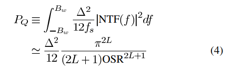
이 값은 OSR이 증가함에 따라 오버샘플링만 사용했을 때(2)보다 약 6L dB/옥타브 더 감소합니다. 이는 오버샘플링과 노이즈 셰이핑의 결합된 작용의 직접적인 결과입니다.
https://ieeexplore.ieee.org/document/5672380
Sigma-Delta Modulators: Tutorial Overview, Design Guide, and State-of-the-Art Survey
This paper presents a tutorial overview of <formula formulatype="inline" xmlns:mml="http://www.w3.org/1998/Math/MathML" xmlns:xlink="http://www.w3.org/1999/xlink"> <tex Notation="TeX">$\Sigma\Delta$</tex></formula> modulators, their operating principles an
ieeexplore.ieee.org
'시스템 반도체 설계 > Sigma-Delta Modulators' 카테고리의 다른 글
| [DSM] 논문 : Sigma-Delta Modulators (4) Nonideal Performance and Systematic Design (1) | 2024.09.13 |
|---|---|
| [DSM] 논문 : Sigma-Delta Modulators (3) Taxonomy of ΣΔ Modulators (1) | 2024.09.12 |
| [DSM] 논문 : Sigma-Delta Modulators (2) Fundamentals of ΣΔ Modulators (1) | 2024.09.11 |
| [ΣΔMs] Sigma-Delta Modulators 의 기본 구조 (0) | 2024.02.28 |
| [ΣΔMs] Sigma-Delta Modulators (1) | 2024.02.27 |


